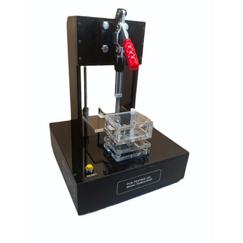
Product Description
To cater to the variegated requirements of the customers, we are engaged in manufacturer and supplier of qualitative range of Low Cost PCBA Functional Dedicated Test Jigs. These are highly appreciated and demanded across the market for their optimum performance and fine finish. These are designed with modern technology and skills to keep it as per set quality standards at production unit. Our valuable clients can avail these Low Cost PCBA Functional Dedicated Test Jigs from us at cost effective prices.
Product Specification
| Country of Origin | Made in India |
| Type | Single |
| Usage | Test |
| Material | Acrylic |
| Phase Type | Single Phase |
| Power Source | Electric |
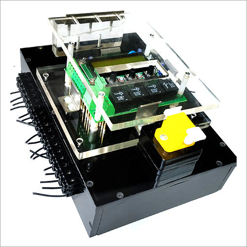
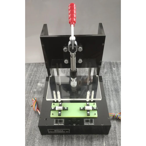
Reliable PCBA Functional TestingThis jig offers repeatable, precise electrical connectivity for USB, UART, and GPIO test points. Spring-loaded gold-plated probes and guided PCB alignment grooves ensure robust contact and minimize false results, ideal for mass production environments.
User-Friendly Design for Quick OperationWith a semi-automatic press-down mechanism and manual loading/unloading, the jig provides an intuitive workflow. Standard dimensions and ergonomic fixture make setup fast and user operation effortless, supporting efficient throughput.
Durable and Safe for Extended UseManufactured from industrial-grade ABS and copper alloy, the fixture sustains up to 100,000 test cycles, featuring overcurrent protection and LED indicators for status feedback. Its stability and safety are enhanced for demanding production lines.
Customizable to Meet Diverse PCB NeedsThe jig's fixture layout can be tailored to different PCBA shapes and sizes, supporting a variety of product lines. Standard 2.54mm pitch and high placement accuracy within 0.1mm ensure compatibility with most test equipment.
FAQ's of Low Cost PCBA Functional Dedicated Test Jigs:
Q: How does the semi-automatic press-down mechanism improve test consistency?
A: The semi-automatic press-down mechanism ensures uniform pressure and consistent contact when engaging test probes with PCBA test points, reducing user error and enhancing repeatability across test cycles.
Q: What types of electrical interfaces does this test jig support?
A: This test jig supports USB, UART, and GPIO test points, making it suitable for verifying functional integrity across multiple communication protocols commonly used in PCBA designs.
Q: When should I consider customizing the fixture layout for my PCBA?
A: Customization is recommended when your PCBA board shape, size, or connector placement differs from standard layouts. The jig can be tailored to accommodate unique board requirements, improving fixture compatibility and test accuracy.
Q: Where is the test jig manufactured and who supplies it?
A: The test jig is manufactured and supplied in India, ensuring local support, rapid turnaround, and reliability for domestic electronics manufacturers and suppliers.
Q: What process is involved in operating this test jig?
A: Operation involves manual placement of the PCBA onto the jig, activating the spring-loaded press mechanism to establish probe contact, and monitoring the LED indicator for test status. Boards are then manually unloaded post-testing.
Q: Is there any benefit to using gold-plated spring-loaded test probes?
A: Gold-plated spring-loaded test probes provide excellent corrosion resistance and highly reliable electrical contact, which improves data accuracy and extends the life of both probes and the PCBA under test.
Q: How does the integrated overcurrent protection enhance safety during testing?
A: The built-in overcurrent protection circuit automatically limits excessive currents during testing, protecting both the PCBA and jig components from damage and offering safe operation for extended use.
 Mon - Sat 8:00 - 6:30


 Contact Us


 Send Inquiry
 Send SMS